


 Instagram
 YouTube
They’re Cool, but How Can We Use Them?
Computation Sheds Light on New Nanostructures
July 1, 2004
Start with a quantum dot — a conglomeration of a few hundreds or thousands of atoms in which it is possible to control a single electron. Attach to the dot four rods of another material which are electronically coupled to the central quantum dot, then have the rods start branching. You’re creating nanocrystals in various shapes that may have useful electronic or optical properties. But how do you find out what those proper- ties are?
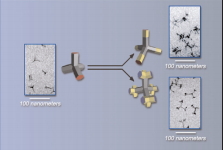
Examples of nanostructures made possible by the Alivisatos group’s new method include tetrapods of cadmium selenide (left) extended with segments of cadmium telluride (upper right), which can be made to branch in turn (lower right).
Ask the computational scientists on your team.
That’s what Paul Alivisatos and his colleagues did. Alivisatos, director of Berkeley Lab’s Materials Sciences Division and professor of chemistry at the University of California at Berkeley, and his research team have demonstrated a general approach for fabricating inorganically coupled colloidal quantum dots and rods. These remarkable new branched struc- tures, whose dimensions are measured in billionths of a meter, are described in the July 8 issue of Nature [1].
Lin-Wang Wang and postdoctoral fellow Jingbo Li of CRD’s Scientific Computing Group have worked closely with the Alivisatos group, using advanced computational techniques to identify the properties of new nanostructures coming out of the laboratory. Calculating the electronic properties of the structures depends on which compounds are involved, how they are joined, the number and arrangement of their atoms, and their proximity to other structures.
Analysis of the current batch of nanocrystals suggests that some of the new composite forms may have future applications in quantum computers, which operate by controlling the coherence (relatedness) of small collections of electron wavefunctions. And the unusual electronic band structures of other forms have possible implications for photovoltaic energy conversion in solar cells.
The Tricky In-Between Scale
Wang defines a nanostructure as “an assembly of building blocks on the scale where their properties become different from their bulk counterparts.” A nanostructure may be composed of anywhere from a few hundred to a million atoms. While existing methods of calculation are well developed for very small collections of atoms, as in a molecule, or very large collections (virtually infinite) in bulk materials, the region in between is where calculations run into problems.

NERSC calculations using local density approximation, the charge patching method, and the fold-
ed spectrum method yield atom-by-atom electronic
maps of a tetrapod with one leg of cadmium selenide and three of cadmium telluride. On the left, green marks the conduction band’s lowest energy state, which is physically separated in the structure from the valence band’s highest energy state, shown in green on the right.
“One would like to use ab initio methods, which start by simply inputting a few atomic numbers and deriving the properties and behavior of the system directly,” Wang says. “The Schrödinger equation theoretically makes that possible, but in practice calculating anything larger than a single helium atom necessarily involves simplifications and approximations.”
Physicists use a modified ab initio technique called the local density approximation (LDA) to calculate the electronic structures of small systems (density refers to the electron charge density in specific regions of the sample).
“Even with LDA, you could spend months doing a straightforward calculation of the electron wavefunctions and their charge densities for a nanosystem with thousands of atoms,” Wang says. The memory needed for calculation increases as the square of the number of atoms in the system — while the needed processing power increases as the cube! A million-atom system is far out of reach of LDA.
So Wang and his colleagues developed a hybrid method, which draws on LDA to determine the charge density in one small region of a crystal, then by “charge patching” extends the charge density to the entire sys- tem, in this case a quantum dot or nanorod.
To accurately model a nanostructure, Wang begins by “passivating” its surface with fractionally charged pseudo-hydrogen atoms — mathematical entities that assign the surface atoms the same reactivity as that of a real nanoparticle in suspension. The positions of the interior atoms are calculated with the valence force field method, which models the strength, elasticity, and direction of bonds among atoms.
Then LDA is used to determine the charge “motifs” around a number of representative atoms, including the surface pseudo-hydrogens. Through charge patching, the calculation is extended to include the entire nanostructure. In a final step, a “folded spectrum” method that Wang developed 10 years ago is used to determine the material’s electronic states near the band gap, including the highest-energy state of the valence band (which in an ideal semiconductor is filled with electrons) and the lowest energy state of the conduction band (which is empty of eletrons).
The various ways that compounds can be assembled into different structures yield very different optical and electronic properties. “The charge-patching method allows us to model thousand-atom structures with ab initio accuracy in about one hour, with the help of the Seaborg supercomputer at NERSC,” says Wang. “This gives us unprecedented power to predict the electronic and optical properties of a given nanostructure.”
Predicting and Tuning the Properties of Nanostructures
The marriage of nanostructure fabrication with the ability to precisely calculate electronic properties opens possibilities for collaboration in more ways than one. “In this case the researchers had already synthesized the structures, and we were able to tell them the electronic properties and how they change with alterations,” Wang says. “In the future, by modeling a proposed system in advance, we could help decide what’s possible and how to control their results.”
The ability to independently tune the properties of each component and the nature of their interactions will enable researchers to create electronic devices tailored to a variety of uses. The structures can be chemically manufactured in large quantities, for potential applications ranging from ultrafast transistors to artificial photosynthesis.
Wang’s research on nanoscale electronic structure calculations has attracted international attention. While continuing to collaborate with the Alivisatos group, Wang is also making his expertise available to users of Berkeley Lab’s new Molecular Foundry (foundry.lbl.gov). One of five DOE Nanoscale Science Research Centers, the Molecular Foundry is focused on the dissemination of techniques and methods for fabricating nanoscale patterned materials. As a computational science liaison to the Foundry’s affiliated theory laboratory, Wang will help Foundry users apply LDA, empirical pseudopotential, and charge patching methods, and will continue working to develop new computational methods to meet the needs of the burgeoning fields of nanoscience and nanotechnology.
About Computing Sciences at Berkeley Lab
High performance computing plays a critical role in scientific discovery. Researchers increasingly rely on advances in computer science, mathematics, computational science, data science, and large-scale computing and networking to increase our understanding of ourselves, our planet, and our universe. Berkeley Lab’s Computing Sciences Area researches, develops, and deploys new foundations, tools, and technologies to meet these needs and to advance research across a broad range of scientific disciplines.