The Challenge of Energy-Efficient HPC
September 11, 2009
The electrical power demands of ultrascale computers threaten to limit the future growth of computational science. To reach exascale computing cost-effectively, a group of researchers propose to radically change the relationship between machines and applications by developing a tightly-coupled hardware/software co-design process. The Green Flash project is intended to dramatically accelerate the development cycle for exascale systems while decreasing the power requirements.
In April, May, and June 2007, three town hall meetings were held at Lawrence Berkeley, Oak Ridge, and Argonne national laboratories to collect community input on the prospects of a proposed new DOE initiative entitled Simulation and Modeling at the Exascale for Energy and the Environment, or E3 for short. About 450 researchers from universities, national laboratories, and U.S. companies discussed the potential benefits of advanced computing at the exascale (1018 operations per second) on global challenge problems in the areas of energy, the environment, and basic science. The findings of the meetings were summarized in a document that quickly became known as the E3 Report.
The E3 Report stated that exascale computer systems are expected to be technologically feasible within the next 15 years, but that they face significant challenges. One of the challenges receiving a great deal of attention throughout the high-performance computing (HPC) community is power efficiency. An exaflop/s system that requires less than 20 megawatts (MW) of sustained power consumption (enough to power approximately 2,600 homes) is “perhaps achievable,” according to the E3 findings, if computers become more power efficient. But if existing technology is simply extrapolated into the future, power estimates grow roughly an order of magnitude higher. When the cost of electricity to run and cool a supercomputer grows to exceed its procurement cost (which is already happening at some major data centers), the economic viability of such projects may come into question.
The electrical power demands of ultrascale computers threaten to limit the future growth of computational science. For decades, the notion of computer performance has been synonymous with raw speed as measured in flop/s (floating point operations per second). That isolated focus has led to supercomputers that consume egregious amounts of electrical power. Other performance metrics—such as power efficiency, space efficiency, reliability, availability, and usability—have been largely ignored. As a consequence, the total cost of ownership of a supercomputer has increased extraordinarily. The current approach to building supercomputers is not sustainable without dramatic increases in funds to operate the systems.
While Moore’s Law—which predicts that the number of transistors per chip will double every 18 months—is alive and well, more transistors are no longer resulting in faster chips that consume less energy. Traditional methods for extracting more performance per processor have been well mined. The only way to improve performance now is to put more cores on a chip. In fact, it is now the number of cores per chip that is doubling every 18 months, instead of clock frequency doubling, as it has in the past.
Consequently, the path towards realizing exascale computing depends on riding a wave of exponentially increasing system concurrency, in which tens to hundreds of processes are executing at the same time—not just within the entire system, as in massively parallel computing, but within each multiple-core processor. This is leading to reconsideration of interconnect design, memory balance, and input/output (I/O) system design. The entire software infrastructure is built on assumptions that are no longer true. The shift to multicore (two, four, or eight cores) and manycore processors (tens to hundreds of cores) will have dramatic consequences for the design of future HPC applications and algorithms.
To reach exascale computing cost-effectively, a group of researchers from the National Energy Research Scientific Computing Center (NERSC) Division and the Computational Research Division (CRD) at Lawrence Berkeley National Laboratory (LBNL, or Berkeley Lab) proposed to radically change the relationship between machines and applications by developing a tightly-coupled hardware/software co-design process.
Their project—named Green Flash after the optical phenomenon that sometimes appears on the horizon at sunset or sunrise—has the aggressive goal of achieving 100 times the computational efficiency and 100 times the capability of the mainstream HPC approach to hardware/software design. We propose to use global cloud system resolving models for climate change simulation as one of the key driver applications to develop the hardware/software co-design methodology. This hardware/software co-design process is intended to dramatically accelerate the development cycle for exascale systems while decreasing the power requirements.
Reducing Waste in Computing
The low-power, embedded-computing market—including consumer electronics products such as cell phones, PDAs, and MP3 players—has been the driver for processor innovation in recent years. The processors in these products are optimized for low power (to lengthen battery life), low cost, and high computational efficiency.
According to Mark Horowitz, Professor of Electrical Engineering and Computer Science at Stanford University and co-founder of Rambus Inc., “Years of research in low-power embedded computing have shown only one design technique to reduce power: reduce waste.” The sources of waste in current HPC systems include wasted transistors (surface area), wasted computation (useless work, speculation, stalls), wasted bandwidth (data movement), and chip designs optimized for serial performance, which increases the complexity (and power waste) of the design.
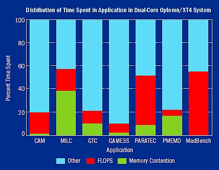
Efficient designs must be specific to application and/or algorithm classes, as suggested by a NERSC/CRD study that examined the dual-core AMD processor used in the Cray XT3 and XT4 systems to assess the current state of system balance and to determine when to invest more resources to improve memory bandwidth. The study used the NERSC SSP benchmark, which is a diverse array of full-scale applications that represent a significant fraction of the NERSC workload. A breakdown of time spent in various components of the codes shows that surprisingly little time could be attributed to memory contention corresponding to basic memory bandwidth limitations (figure 1). The largest fraction of time (the “Other” category) is attributed to either latency stalls or integer/address arithmetic. Theoretically, these applications should all be memory-bandwidth bound, but instead the study shows that most are constrained by other microarchitectural bottlenecks in existing processors, and that different applications have different balance requirements.

Figure 1. A breakdown of where time was spent in a subset of the NERSC SSP application codes suggests that different applications have different requirements for computational efficiency.
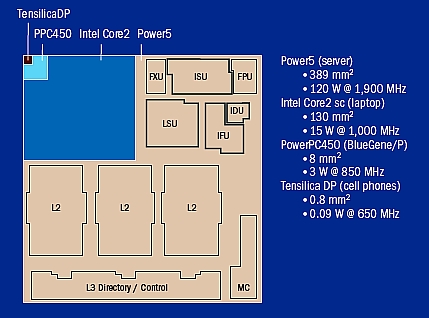
A core designed to a specific set of application resource requirements can get 10–100 times better performance per watt, as shown by studies from Stanford University and from Tensilica Inc. Figure 2 (p51) illustrates this potential by showing the area and performance differences between general purpose, embedded (used in IBM’s BlueGene/P), and application-tailored cores. The figure shows how much area and power desktop processors waste because they are optimized for serial code. The DOE’s science applications, because they are already highly parallel, are an excellent driver for understanding how processors can be designed to optimize for efficient parallel execution rather than serial execution.

Figure 2. Relative size and power dissipation of different CPU core architectures. Simpler processor cores require far less surface area and power with only a modest drop in clock frequency. Even if measured by sustained performance on applications, the power efficiency and performance per unit area is significantly better when using the simpler cores.
Parallelism is an energy-efficient way to achieve performance. A system with many simple cores offers higher performance per unit area for parallel codes than a comparable design employing smaller numbers of complex cores. Lower complexity makes a chip more economical to design and produce, and smaller processing elements provide an economical way to improve defect tolerance by providing many redundant cores that can be turned off if there are defects.
Figure 2 (p51) shows that moving to a simpler core design results in modestly lower clock frequencies, but has enormous benefits in chip surface area and power consumption. Even if it is assumed that the simpler core will offer only one-third the computational efficiency of the more complex out-of-order cores, a manycore design could still provide an order of magnitude more power efficiency for an equivalent sustained performance. As the figure illustrates, even with the smaller cores operating at one-third to one-tenth the efficiency of the largest chip, 100 times more cores can still be packed onto a chip and consume one-twentieth the power. Effective performance per watt is the critical metric.
This design approach brings with it an even greater challenge: creating ultrascale parallel applications that can run effectively on this radically different architecture.
A Hardware/Software Co-Design Process
If the HPC community emulated the embedded computing industry, we could potentially reduce not only power requirements but also design costs and time to market. A key limiting factor in the market-driven approach to HPC procurements is the length of the feedback loop on system designs. Due to the high design investment cost, the vendor must make compromises in the system design to accommodate a wide variety of applications. The application scientists cannot provide performance feedback to the vendor until hardware is released for testing and evaluation. This multi-year cycle is a source of significant inefficiencies for scientific productivity, because it can take years for each new iteration of hardware to become available for testing and evaluation by the application scientists. A hardware/software co-design approach could dramatically accelerate this process.
For years, NERSC has engaged in a cooperative effort with hardware designers called Science-Driven System Architecture, which involves engaging application scientists in the early stages of the hardware design process for future-generation supercomputing systems. The Green Flash team is currently focusing this cooperative effort toward a new design paradigm: application-driven HPC. This approach involves identifying high-impact exascale scientific applications, tailoring the system architecture to the application resource requirements, and co-designing algorithms and software together with the semi-custom hardware.
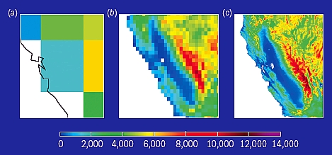
The first application to be chosen for the approach is the geodesic global cloud-resolving model (GCRM) being developed by David Randall and his group at Colorado State University (CSU), where he is Director of the Center for Multiscale Modeling of Atmospheric Processes and principal investigator of the DOE SciDAC project “Design and Testing of a Global Cloud-Resolving Model” (sidebar “Global Cloud Resolving Models”). Although the current SciDAC project aims to develop a cloud model with a 3 km horizontal grid resolution, the ultimate goal is 1 km resolution, which would allow researchers to replace the statistical approximations of cumulus convective cloud systems used in current climate models with direct numerical simulations of individual cloud systems, providing more precise modeling of heat and moisture transport (figure 3).

Figure 3. Topography of California and Nevada at three different model resolutions. The left panel shows the relatively low resolution typical of the models used for the International Panel on Climate Change’s Fourth Assessment Report, published in 2006. The center panel shows the upper limit of current climate models with statistical approximations of cloud systems. The right panel shows the resolution needed for direct numerical simulation of individual cloud systems.
To develop a 1 km cloud model, scientists would need a supercomputer that is 1,000 times more powerful than what is available today. But building a supercomputer that powerful with conventional microprocessors (the kind used to build personal computers) would cost about $1 billion and would require 200 megawatts of electricity to operate—enough energy to power a small city of 100,000 residents.
The Green Flash system will employ power-efficient cores specifically tailored to meet the requirements of this ultrascale climate code. The requirements of an atmospheric model at 1 km resolution are dominated by the equations of motion because the Courant stability condition requires smaller time steps. To be useful for projections of future climate change, the model must run at least 1,000 times faster than real time, calculating values for about two billion icosahedral points. At this rate, millennium-scale control runs could be completed in a year, and century-scale transient runs could be done in a month. The computational platform’s sustained performance would need to reach at least 10 petaflop/s. This goal could be achieved with 20 million processors (consuming less than 4 MW of power), modest vertical parallelization, a modest speed of 0.5 gigaflop/s per processor, and 5 MB memory per processor.
An application-driven architecture does not necessitate a special-purpose machine, nor does it require exotic technology. As figure 6 shows with several examples, there is a customization continuum from general-purpose to single-purpose computers, and indeed the IBM Blue Gene line of systems was started with a very narrow application target in mind.

Figure 6. The customization continuum of computer architectures.
At the single-purpose, fully custom extreme is MD-Grape, a computer at RIKEN in Japan. MD-Grape was custom designed for molecular dynamics simulations (the name stands for “Molecular Dynamics-Greatly Reduced Array of Processor Elements”) and has an application-specific integrated circuit (ASIC) chip design. It achieves 1 petaflop/s performance for its target application using 200 kilowatts of power, and cost $8.6 million from concept to implementation (including labor). Although MD-Grape was custom designed for molecular dynamics, it has proven useful for several other applications, including astrophysical N-body simulations.
An example of a semicustom design with some custom elements is the D. E. Shaw system. D. E. Shaw Research, a unit of an investment firm, focuses on the development of new algorithms and specialized supercomputer architectures for ultra-fast biomolecular simulations of scientific and pharmaceutical problems. The D. E. Shaw system uses fully programmable cores with full-custom co-processors to achieve efficiency, and simulates 100–1,000 times longer timescales than any other HPC system. While the programmability of the D. E. Shaw system broadens its application reach, it is still narrower than Berkeley Lab’s Green Flash.
IBM’s Blue Gene is the best example to date of the kind of application-driven architecture based on an embedded processor core that the Green Flash project envisions. Designed around a protein folding application, Blue Gene, over several generations, has proved to be useful for a growing list of applications, including hydrodynamics, quantum chemistry, molecular dynamics, climate modeling, and financial modeling.
Like Blue Gene, the Green Flash system will have a semicustom design. The core architecture will be highly programmable using C, C++, or Fortran. Its projected 100 times improvement in power efficiency would be modest when compared with the demonstrated capability of more specialized approaches. This approach will solve an exascale problem without building an exaflop/s machine.
The hardware/software co-design process would be impossible using the typical multi-year hardware lead times for complex, serial-optimized chips. However, a typical embedded processor vendor may generate up to 200 unique designs every year for simple, specialized chips. In order to keep up with the demand for semi-customized designs, leading embedded-design houses—such as IBM Microelectronics, Altera, and Tensilica—have evolved sophisticated toolsets to accelerate the design process through semi-automated synthesis of custom processor designs. We are now leveraging the expertise of this technology sector by collaborating with Mark Horowitz of Stanford University and Rambus, Inc., and Chris Rowen of Tensilica Inc.
Our co-design process utilizes the Research Accelerator for Multiple Processors (RAMP), an emulation platform that makes the hardware configuration available for evaluation while the actual hardware is still on the drawing board (sidebar “RAMP: Hardware Emulation for Rapid Prototyping”). The flexibility of RAMP allows rapid changes in the details of the hardware configuration, making hardware/software co-design feasible. In fact, we have recently demonstrated a 30%–50% improvement in power efficiency over conventional approaches to design space exploration.
The software side of the co-design process is supported by auto-tuning tools for code generation that are being developed by the SciDAC Center for Scalable Application Development Software (CScADS), led by John Mellor-Crummey of Rice University (sidebar “Auto-Tuning for Chip Multiprocessors”).
In addition to enabling a breakthrough in cloud-resolving climate simulation, Green Flash’s power-efficient, application-driven design methodology will have an impact on the broader DOE scientific workload. This hardware/software co-design approach is geared for a class of codes, not just for a single code instantiation, so this methodology is broadly applicable and could be extended to other scientific disciplines. Blue Gene was originally targeted at chemistry and bioinformatics applications, resulting in a power-efficient architecture, but its application has been broader than the original target. A similar result is expected from Green Flash.
First Prototype Runs Successfully
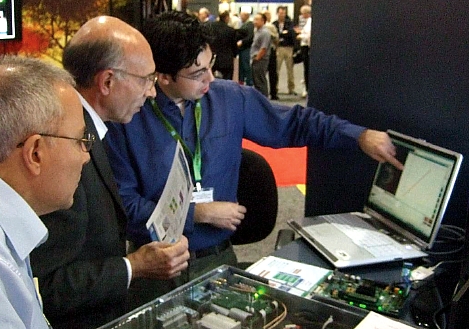
The Green Flash project has successfully reached its first milestone by running a next-generation, limited area model version of the GCRM on a logical prototype of a Green Flash processor. The logical prototype, which simulates the entire circuit design of the proposed processor, was designed in collaboration with Tensilica, using Tensilica’s Xtensa LX extensible processor core as the basic building block, and was run on a RAMP BEE3 hardware emulator. A demonstration of the prototype ran at the SC08 conference in Austin, Texas in November 2008 (figure 12).

Figure 12. David Donofrio of LBNL demonstrates the Colorado State University limitedarea geodesic climate model running on RAMP at Supercomputing 2008. The RAMP BEE3 board (in the foreground) is running a cycle-accurate circuit-level simulation of the science application-optimized embedded processor core that would be used in the Green Flash system. The simulation runs at 100 MHz, which is only five times slower than the target clock frequency of 500 MHz. RAMP enables early evaluation of systems using full applications, whereas software simulation forces researchers to make design decisions based on small extracted kernels.
The hardware goals for the prototype research are fairly simple: produce a hardware prototype of a single Green Flash processor by fall 2009, and an entire node of the system (64 to 128 processors) by fall 2010. But the software goals are more challenging. There are open issues that we are still wrestling with. We know how to program embedded processors for the GCRM code, but we have not fully explored the more general question of how to program a machine with 20 million processors. But by examining this one particular case, we hope to learn lessons that can be generalized to other codes with similar algorithms on a machine of this scale. Whether or not a full-scale Green Flash system is built, the answers to these questions will be the most important research challenges for the computer science community for the next decade.
Contributors
Dr. John Shalf, NERSC Division, LBNL; Dr. Michael Wehner and Dr. Leonid Oliker, Computational Research Division, LBNL; John Hules, Computing Sciences Communications, LBNL
Acknowledgements
Green Flash is funded by the LBNL Laboratory Directed Research and Development program. All authors from LBNL were supported by the Office of Advanced Scientific Computing Research or the Climate Change Prediction Program under the Office of Biological and Environmental Research in the Department of Energy Office of Science under contract number DE-AC02-05CH11231
Further Reading
Green Flash
http://www.lbl.gov/CS/html/greenflash.html
About Computing Sciences at Berkeley Lab
High performance computing plays a critical role in scientific discovery. Researchers increasingly rely on advances in computer science, mathematics, computational science, data science, and large-scale computing and networking to increase our understanding of ourselves, our planet, and our universe. Berkeley Lab’s Computing Sciences Area researches, develops, and deploys new foundations, tools, and technologies to meet these needs and to advance research across a broad range of scientific disciplines.


 Instagram
 YouTube