The MANYCORE Revolution: Will HPC LEAD or FOLLOW?
September 11, 2009
The MANYCORE Revolution: Will HPD LEAD or FOLLOW?
Rumors of the death of Moore’s Law are greatly exaggerated, according to a team of computer scientists from Lawrence Berkeley National Laboratory (LBNL) and the University of California (UC)–Berkeley. In their view, Gordon Moore’s observation that the amount of computing power packed onto a chip doubles about every 18 months while the cost remains flat is alive and well. But the physics is changing.
Industry clung to the single-core model for as long as possible, arguably over-engineering the cores to eke out a few percentage points of increased performance. But the complex core designs of the past required enormous area, power, and complexity to maximize serial performance. Now, heat density and power constraints have all but ended 15 years of exponential clock frequency growth. The industry has responded by halting clock rate improvements and increases in core sophistication, and is instead doubling the number of cores every 18 months. The incremental path towards “multicore” chips (two, four, or eight cores) has already forced the software industry to take the daunting leap into explicit parallelism. Once you give up on serial code, it is much easier to take the leap towards higher degrees of parallelism—perhaps hundreds of threads. If you can express more parallelism efficiently, it opens up a more aggressive approach, termed “manycore,” that uses much simpler, lower-frequency cores to achieve more substantial power and performance benefits than can be achieved by the incremental path. With the manycore design point, hundreds to thousands of computational threads per chip are possible. Ultimately, all of these paths lead us into an era of exponential growth in explicit parallelism.
However, fully unleashing the potential of the manycore approach to ensure future advances in sustained computational performance will require fundamental advances in computer architecture and programming models—advances that are nothing short of reinventing computing. This in turn will result in a new parallel programming paradigm, which is already being explored by Berkeley researchers in a five-year program funded by Microsoft, Intel, and California’s UC Discovery program.
Recent trends in the microprocessor industry have important ramifications for the design of the next generation of high-performance computing (HPC) systems as we look beyond the petascale. The need to switch to an exponential growth path in system concurrency is leading to reconsideration of interconnect design, memory balance, and I/O system design that will have dramatic consequences for the design of future HPC applications and algorithms. The required reengineering of existing application codes will likely be as dramatic as the migration from vector HPC systems to massively parallel processors (MPPs) that occurred in the early 1990s. Such comprehensive code re-engineering took nearly a decade for the HPC community, so there are serious concerns about undertaking yet another major transition in our software infrastructure. However, the mainstream desktop and handheld computing industry has even less experience with parallelism than the HPC community. The transition to explicit on-chip parallelism has proceeded without any strategy in place for writing parallel software.
Although industry is making moves in this direction and starting to get its feet wet, the HPC community has yet to take up the cause. But as one member of the Berkeley team puts it, “To move forward in HPC, we’re all going to have to get on the parallelism crazy train.”
The Berkeley team laid out their ideas in a paper entitled “A View of the Parallel Computing Landscape” published in late 2006. Known informally as “The Berkeley View,” the paper continues to draw interest and spur discussion. When co-author David Patterson of UC–Berkeley presented an overview at the SC08 conference in Austin in November 2008, hundreds of attendees turned out for his invited talk, which addressed “the multicore/manycore sea change.”
A Shift Driven by Industry
The trend toward parallelism is already underway as the industry moves to multicores. Desktop systems featuring dual-core processors and even HPC are getting in on the act. In the past year, the Cray XT supercomputers at Oak Ridge National Laboratory (ORNL) and NERSC were upgraded from dual-core to quad-core processors. The upgrade not only doubled the number of cores, it also doubled parallelism of the SIMD floating-point units to get a net 3.5× increase in peak flop rate for a 2× increase in core count. While these swaps were relatively quick paths to dramatic increases in performance, the conventional multicore approach (two, four, and even eight cores) adopted by the computing industry will eventually hit a performance plateau, just as traditional sources of performance improvements such as instruction-level parallelism (ILP) and clock frequency scaling have been flattening since 2003, as shown in figure 1.
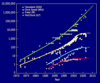
Figure 1. This graph shows that Moore’s law is alive and well, but the traditional sources of performance improvements (ILP and clock frequencies) have all been flattening.

Figure 2. The performance of processors as measured by SpecINT has grown 52% per year with remarkable consistency, but improvements tapered off around 2002.
Figure 2 shows the improvements in processor performance as measured by the SPEC integer benchmark over the period from 1975 to present. Since 1986 performance has improved by 52% per year with remarkable consistency. During that period, as process geometries scaled downward according to Moore’s Law, the active capacitance of circuits and supply voltages also scaled down. This approach, known as constant electric field frequency scaling, fed the relentless increases in CPU clock rates over the past decade and a half. As manufacturers have shrunk chip features below the 90 nm scale, however, this technique began to hit its limits as the transistor threshold voltage could not be scaled ideally without losing large amounts of power to leakage, and this in turn meant the supply voltage could not be reduced correspondingly. Processors soon started hitting a power wall, as adding more power- hungry transistors to a core gave only incremental improvements in serial performance—all in a bid to avoid exposing the programmer to explicit parallelism. Some chip designs, such as the Intel Tejas, were ultimately cancelled due to power consumption issues.
“With the desktop, the mantra was performance at any cost and there really was no interest in computational efficiency—brute force won the day,” says John Shalf of LBNL. “But the move to multicore shows that computational efficiency matters once again.”
This issue of power density has now become the dominant constraint in the design of new processing elements, and ultimately limits clock frequency growth for future microprocessors. The direct result has been a stall in clock frequency that is reflected in the flattening of the performance growth rates starting in 2002. In 2006, individual processor cores are nearly a factor of three slower than if progress had continued at the historical rate of the preceding decade. This has led to a significant course correction in the IT semiconductor roadmap, as shown in figure 3.
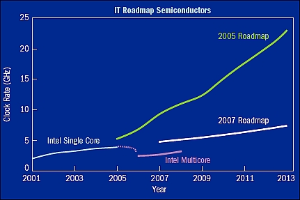
Figure 3. Even some experts in the field were taken by surprise with the sudden end of clock speed scaling. This graph shows the roadmap for processor performance from the International Technology Roadmap for Semiconductors (ITRS), which has been remarkably accurate in their predictions, until recently. In 2005, the group predicted clock rates of over 12 GHz by 2009, but the 2007 roadmap dramatically curtailed those predictions and put them close to what Intel, among other companies, were producing by then.
Other approaches for extracting more performance such as out-of-order instruction processing to increase ILP have also delivered diminishing returns (figure 1, p41). Having exhausted other well-understood avenues to extract more performance from a uniprocessor, the mainstream microprocessor industry has responded by halting further improvements in clock frequency and increasing the number of cores on the chip. In fact, as Patterson noted in his presentation at the SC08 conference in Austin, AMD, Intel, IBM, and Sun now sell more multicore chips than uniprocessor chips. Whether or not users are ready for the new processors, Patterson and John Hennessy—President of Stanford and co-author of the famous architecture textbook with Patterson—estimate the number of cores per chip is likely to double every 18–24 months henceforth. Hennessy has commented, “if I were still in the computing industry, I’d be very worried right now.” New chips currently on the drawing boards and which will appear over the next five years are parallel, Patterson notes. Therefore, new algorithms and programming models will need to stay ahead of a wave of geometrically increasing system concurrency—a tsunami of parallelism.
The stall in clock frequencies and the industry’s comparatively straightforward response of doubling cores has reinvigorated study of more radical alternative approaches to computing such as Field-Programmable Gate Arrays (FPGAs), general-purpose programming of Graphics Processing Units (GPGPUs), and even dataflow-like tiled array architectures such as the TRIPS project at the University of Texas–Austin. The principal impediment to adapting a more radical approach to hardware architecture is that we know even less about how to program efficiently such devices for diverse applications than we do parallel machines composed of multiple CPU cores. Kurt Keutzer puts this more elegantly when he states, “The shift toward increasing parallelism is not a triumphant stride forward based on breakthroughs in novel software and architectures for parallelism; instead, this plunge into parallelism is actually a retreat from even greater challenges that thwart efficient silicon implementation of traditional uniprocessor architectures.” To get at the heart of Keutzer’s statement, it is necessary to deconstruct the most serious problems with current CPU core designs.
New IC Design Constraints
The problem of current leakage, which limits continued performance improvements based on clock frequency scaling, is not the only constraint helping to push the semiconductor industry in new directions. The other problem facing the industry is the extremely high cost of new logic designs, which creates pressure to simplify and shrink core designs. In order to squeeze more performance out of processor cores at high frequencies, a considerable amount of surface area is devoted to latency hiding technology, such as deep execution pipelines and out-of-order instruction processing. The phenomenally complex logic required to implement such features has caused design costs of new chips to skyrocket to hundreds of millions of dollars per design. It has also become impractical to verify all logic on new chip designs containing hundreds of millions of logic gates due to the combinatorial nature of the verification process. Finally, with the move to smaller feature sizes for future chips, the likelihood of chip defects will continue to increase, and any defect makes the core that contains it non-functional. Larger and more complex CPU logic designs place a higher penalty on such defects, thereby lowering chip yield. Industry can and does sell chips in which a core is disabled, but such chips are more attractive if the missing core is a small fraction of the overall performance. These key problems ultimately conspire to limit the performance and practicality of extrapolating past design techniques to future chip designs, regardless of whether the logic implements some exotic non-von Neumann architecture, or a more conventional approach.
In the view of the Berkeley team, here are the remedies for these problems:
- Power—parallelism is an energy-efficient way to achieve performance. Many simple cores offer higher performance per unit area for parallel codes than a comparable design employing smaller numbers of complex cores.
- Design Cost—the behavior of a smaller, simpler processing element is much easier to predict within existing electronic design-automation workflows and more amenable to formal verification. Lower complexity makes the chip more economical to design and produce.
- Defect Tolerance—smaller processing elements provide an economical way to improve defect tolerance by providing many redundant cores that can be turned off if there are defects. For example, the Cisco Metro chip contains 188 cores with four redundant processor cores per die. The STI Cell processor has eight cores, but only six are enabled in its mainstream consumer application—the Sony PlayStation 3—in order to provide additional redundancy to better tolerate defects.
Getting Around the Constraints: Manycore versus Multicore
The industry buzzword “multicore” captures the plan of doubling the number of standard cores per die with every semiconductor process generation starting with a single processor. Multicore will obviously help multiprogrammed workloads, which contain a mix of independent sequential tasks, and prevent further degradation of individual task performance. But how will individual tasks become faster? Switching from sequential to modestly parallel computing will make programming much more difficult without rewarding this greater effort with a dramatic improvement in power-performance. Hence, multicore is unlikely to be the ideal answer.
The alternative approach moving forward is to adopt the “manycore” trajectory, which employs simpler cores running at modestly lower clock frequencies. Rather than progressing from two to four to eight cores with the multicore approach, a manycore design would start with hundreds of cores and progress geometrically to thousands of cores over time. Figure 4 shows that moving to a simpler core design results in modestly lower clock frequencies, but has enormous benefits in power consumption and chip surface area. Even if you presume that the simpler core will offer only one-third the computational efficiency of the more complex out-of-order cores, a manycore design would still be an order of magnitude more power- and area-efficient in terms of sustained performance.
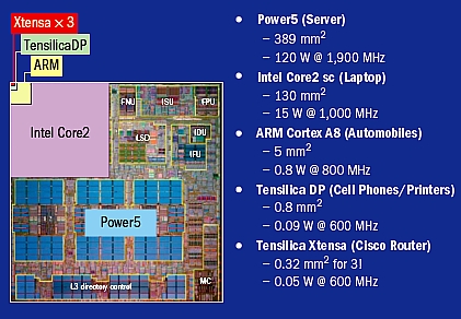
Figure 4. The diagram shows the relative size and power dissipation of different CPU core architectures. Simpler processor cores require far less surface area and power with only a modest drop in clock frequency. Even if measured by sustained performance on applications, the power efficiency and performance per unit area is significantly better when using the simpler cores.
Consumer Electronics Core Design Meets High-End Computing
The approach of using simpler lower-frequency core designs has been used for many years by the embedded-computing industry to improve battery life, lower design costs, and reduce time to market for consumer electronics. In the past the design targets for embedded applications were nearly the opposite of the performance-driven requirements of high-end computing. However, the needs of the high-end computing market have converged with the design motivation of the embedded-computing industry as a result of their common need to improve energy efficiency and reduce design costs. With regard to energy efficiency, the embedded-computing industry has the most accumulated expertise and technology. Whereas past design innovations in high-end computing, such as superscalar execution and out-of-order instruction pipelines, trickled down to consumer applications on PCs, we are starting to see innovations that emerged in the embedded space trickling up into high-end server designs. This flow of innovation is likely to increase in the future.
Designing a core that does no more than you need it to do makes sense and the tools used to design embedded chips revolve around tailoring the core design for the specific application. This really changes the meaning of “commodity computing technology,” from repurposing a complete computer node designed for a broader desktop market to repurposing a core designed for a broader consumer electronics market—it takes the meaning of commodity and moves it onto the chip.
The Revolution is Already Underway
There are already examples of the convergence between embedded computing and HPC in the design of the Blue Gene and SiCortex supercomputers, which are based on embedded-processor cores that are more typically seen in automobiles, cell phones, and toaster ovens. Parallelism with concurrencies that have formerly been associated with HPC applications are already emerging in mainstream embedded applications. The Metro chip in new Cisco CRS-1 router contains 188 general-purpose Tensilica cores, and has supplanted Cisco’s previous approach of employing custom Application-Specific Integrated Circuits (ASICs) for the same purpose.
Surprisingly, the performance and power efficiency of the Metro for its application are competitive with full-custom ASIC, which themselves are more power- and area-efficient than could be achieved using FPGAs (dimming hopes that FPGAs offer a more energy efficient approach to computation). The Motorola Razor cell phone also contains eight Tensilica cores. The NVidia G80 (CUDA) GPU replaces the semi-custom pipelines of previous generation GPUs with 128 more general-purpose CPU cores. The G80 in particular heralds the convergence of manycore with mainstream computing applications. Whereas traditional GPGPUs have a remarkably obtuse programming model involving drawing an image of your data to the framebuffer (the screen), the G80’s more general-purpose cores can be programmed using more conventional C code and will soon support IEEE-standard double-precision arithmetic.
The motivation for using more general-purpose cores is the increasing role of GPUs for accelerating commonly required non-graphical game calculations such as artificial intelligence (AI) for characters in games, object interactions, and even models for physical processes. Companies such as AISeek’s Intia and Ageia’s (recently acquired by NVidia) PhysX have implemented game physics acceleration on GPUs that use algorithms that are very similar to those used for scientific simulation and modeling (Further Reading, p49). ATI (recently acquired by AMD) has proposed offering GPUs that share the same cache-coherent HyperTransport fabric of their mainstream CPUs. Intel’s experimental Polaris chip uses 80 simpler CPU cores on a single chip to deliver one teraflop/s of peak performance while consuming only 65 watts and this design experience may feed into future GPU designs from Intel. Both Intel and AMD roadmaps indicate that tighter integration between GPUs and CPUs is the likely path toward introducing manycore processing to mainstream consumer applications on desktop and laptop computers.
Step Aside PCs—Consumer Electronics Are Now Driving CPU Innovation
Taking a historical perspective on HPC system design, Bell’s Law is likely as important to the development of HPC system design as Moore’s Law. Bell’s Law is the corollary of Moore’s Law and holds that by maintaining the same design complexity you can halve the size and costs of the chip every 18 months. The TOP500 project has documented a steady progression from the early years of supercomputing, from exotic and specialized designs towards clusters composed of components derived from consumer PC applications. The enormous volumes and profits of desktop PC technology led to huge cost/performance benefits for employing clusters of desktop CPU designs for scientific applications despite the lower computational efficiency. As we move in to the new century, the center of gravity for the market in terms of unit volume and profit has shifted to handheld consumer electronics. This movement has some significant implications for the future of the HPC.
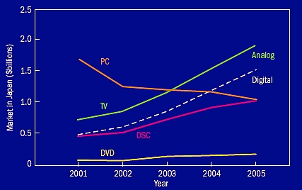
Figure 5. The graph shows the declining influence of PC microprocessors on the overall revenue share in microprocessor-based electronic designs.
As can be seen in figure 5, the market share of the consumer electronics applications for CPUs surpassed that of the desktop PC industry in 2003 and the disparity continues to grow. Shortly after 2003, revenue in the PC business flattened (figure 6), and IBM subsequently sold off its desktop and portable personal computer units. During that same period, Apple moved into the portable electronic music player market with the iPod, then into the cellular phone business and eventually dropped “Computer” from its corporate name. This may be the most dramatic twist yet for the HPC industry if these trends continue (and they likely will). Although the desktop computing industry has been leading a major upheaval in HPC system design over the past decade (the movement to clusters based on desktop technology), that industry segment is no longer in the driver’s seat for the next revolution in CPU design. Rather, the market volume, and hence design targets, are now driven by the needs of handheld consumer electronics such as digital cameras, cell phones, and other devices based on embedded processors.
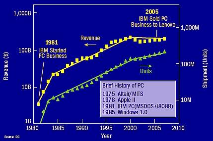
Figure 6. This graph shows how revenues for IBM’s PC business have flattened in response to the increasing dominance of consumer electronics applications in the electronics industry.
The next generation of desktop systems, and consequent HPC system designs, will borrow many design elements and components from the consumer electronics devices. Namely, the base unit of integration for constructing new chip designs targeted at different applications will be the CPU cores derived from embedded applications rather than the transistor. Simpler CPU cores may be combined together with some specialization to HPC applications (such as different memory controllers and double-precision floating point), just as transistors are currently arranged to form current CPU designs. Indeed, within the next three years, there will be manycore chip designs that contain more than 2,000 CPU cores, which is very close to the number of transistors that was used in the very first Intel 4004 CPU. This led Chris Rowen, CEO of Tensilica, to describe the new design trend by saying “the processor is the new transistor.” This is a brave new world, and we do not know where it will take us.
Ramifications for the HPC Ecosystem
Given current trends, petascale systems delivered in 2011 are projected to have the following characteristics:
- Systems will contain between 400,000 and 1,500,00 processors (50,000 to 200,000 sockets). Each socket in the system will be a chip that contains multiple cores.
- In 2011 these multicore chips will contain between 8 and 32 conventional processor cores per chip. Technology based on manycore will employ hundreds to thousands of CPU cores per chip. Consider that the Cisco CRS-1 router currently employs a chip containing 188 processor cores using conventional silicon process technology, so “1,000 cores on a chip” is not as far off as one might expect. A System on Chip (SoC) design, such as Blue Gene or SiCortex, may still use the simpler embedded cores (manycore design point), but sacrifice raw core count to integrate more system services onto the chip (such as interconnect fabric and memory controllers).
- As microprocessor manufacturers move their design targets from peak clock rate to reducing power consumption and packing more cores per chip, there will be a commensurate trend towards simplifying the core design. This is already evidenced by the architecture of the Intel Core-Duo processors that use pipelines that are considerably shorter than those of its predecessor, the Pentium4. The trend towards simpler processor cores will likely simplify performance tuning, but will also result in lower sustained performance per core as out-of-order instruction processing is dropped in favor of smaller, less complex and less power-hungry in-order core designs. Ultimately this trend portends a convergence between the manycore and multicore design points.
- As the number of cores per socket increase, memory will become proportionally more expensive and power hungry in comparison to the processors. Consequently, cost and power-efficiency considerations will push memory balance (in terms of the quantity of memory put on each node) from the current nominal level of 0.5 bytes of DRAM memory per peak flop, down below 0.1 bytes/flop (possibly even less than 0.02 bytes/flop).
- Cost scaling issues will force fully-connected interconnect topologies, such as the fat-tree and crossbar, to be gradually supplanted at the high end by lower-degree interconnects such as the n-dimensional torii, meshes, or alternative approaches, such as hierarchical fully-connected graphs.
The consequence will be that HPC software designers must take interconnect topology and associated increased non-uniformity in bandwidth and latency into account for both algorithm design and job mapping. Currently, the interconnect topology is typically ignored by mainstream code and algorithm implementations. Blue Gene/L programmers already have to grapple with the topology mapping issues—it is merely a harbinger of the broader challenges facing all HPC programmers in the near future. Programming models that continue to present the illusion of a flat system communication cost will offer increasingly poor computational efficiency.
Whether the HPC community is convinced or not that the future is in multicore or manycore technology, the industry has already retooled to move in the direction of geometrically scaling parallelism. If the levels of concurrency that result from a transition directly to manycore appear daunting, the trends on the TOP500 list in figure 7 show that within just three years multicore will take us to the same breathtaking levels of parallelism. With either path, the HPC community faces an unprecedented challenge to existing design practices for system design, OS design, and our programming model. The issue of programmability looms large as computer scientists wonder how on Earth will they stay abreast of exponentially increasing parallelism? If no one can program a manycore computer system productively, efficiently and correctly, then there is little benefit to this approach for maintaining historical per-socket performance improvements for future HPC systems.
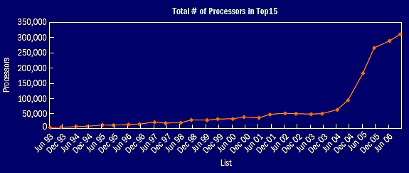
Figure 7. The graph shows the dramatic increase in system concurrency for the Top 15 systems in the annual TOP500 list of HPC systems. Even if BG/L systems are removed from consideration, the inflection point of system concurrency is still quite dramatic.
Time to Get with the Programming
Keeping abreast of geometrically increasing concurrency is certainly the most daunting challenge as we move beyond the petascale in the next few years. Most HPC algorithms and software implementations are built on the premise that concurrency is coarse-grained and its degree will continue to increase modestly, just as it has over the past 15 years. The exponentially increasing concurrency throws all of those assumptions into question. At a minimum, we will need to embark upon a campaign of re-engineering our software infrastructure that may be as dramatic and broad in scope as the transition from vector systems to massively parallel processors (MPPs) that occurred in the early 1990s.
However, the heir apparent to current programming practice is not obvious, in large part because the architectural targets are not clear. There are two major questions, one involving off-chip memory bandwidth and access mechanisms, and the second being organization of the on-chip cores. Some of the initial forays into multicore have kept both of theses issues at bay. For example, the upgrades from dual- to quad-core processors at NERSC and ORNL (figure 8) upgraded memory density and bandwidth at the same time, and the cores were familiar x86 architectures. So using each core as an MPI processor was a reasonable strategy both before and after the upgrades. As with the introduction of shared-memory nodes into clusters in the late 1990s, the message-passing model continued to work well both within and between nodes, which has allowed programmers to avoid rewriting their codes to take advantage of the changes. The reason? The architectures were still relatively hefty cores with their own caches, floating-point units and superscalar support, so programs were best designed with coarse-grained parallelism and good locality to avoid cache coherence traffic. But the incremental changes to chip architecture seen to date may give HPC programmers a false sense of security.
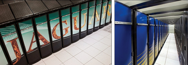
Figure 8. In the past year the Cray XT supercomputers at ORNL (Jaguar, left) and NERSC (Franklin, right) have both been upgraded from dual- to quad-core processors.
Limited off-chip bandwidth—sometimes referred to as the “memory wall”—has been a problem for memory-intensive computations even on single-core chips that predate the move to multicore. The shift to multiple cores is significant only because it continues the increase in total on-chip computational capability after the end of clock frequency scaling allowing us to continue hurtling towards the memory wall. The memory bandwidth problem is as much economic as technical, so the HPC community will continue to be dependent on how the commodity market will move. Current designs are unlikely to sustain the per core bandwidth of previous generations, especially for irregular memory access patterns that arise in many important applications. Even the internal architecture of memory chips is not organized for efficient irregular word-oriented accesses.
There are promising avenues to sustain the growth in bandwidth, such as chip stacking and photonic interfaces, but this will require economic pressure from the mass market to make it happen. That pressure will depend on what applications will drive consumers to buy manycore chips and whether those applications are written in a manner that requires high bandwidth in a form that is usable by the HPC community. A new parallel computing laboratory at Berkeley is working on parallel applications for handheld devices and laptops, and these have revealed some of the same memory bandwidth needs as scientific applications, which means the HPC community will not be on its own in pushing for more bandwidth. For both HPC and consumer applications, the first problem is to make the bandwidth available to the applications through a set of optimizations that mask the other memory system issue—latency. The Berkeley group applies automatic performance tuning techniques to maximize effective use of the bandwidth through latency-masking techniques such as pre-fetching, and is planning on technology innovations to supply the necessary bandwidth. But to hedge their bets on the bandwidth problem, they are also developing a new class of communication-avoiding algorithms that reduce memory bandwidth requirements by rethinking the algorithms from the numerics down to the memory accesses (sidebar “Dwarfs” p48).
The architectural organization question is even more critical to the future of MPI. The notion of a core as a traditional processor may not be the right building block. Instead, the exponentially growing concurrency may come from wider SIMD or vector units, multithreaded architectures that share much of the hardware state between threads, very simple processor cores, or processors with software-managed memory hierarchies. MPI expresses coarse-grained parallelism but is not helpful in code vectorization (or SIMDization). Even if there are many full-fledged cores on a chip, the memory overhead of MPI may make it an impractical model for manycore. Consider a simple nearest-neighbor computation on a 3D mesh—if each of the manycores holds a 10×10×10 subgrid, roughly half of the points are on the surface and will be replicated on neighboring cores. Similarly, any globally shared state will have to be replicated across all cores, because MPI does not permit direct access to shared copies. This has reopened consideration of the hybrid OpenMP+MPI programming model, although that model has shown more failures than successes over the past decade. The problems with the hybrid model have included the lack of locality control in OpenMP, and the interaction between the multiple threads within OpenMP communicating through a shared network resource to other nodes. Even if these deficiencies can be overcome, OpenMP’s use of serial execution as the default between loops will be increasing stymied by Amdahl’s law at higher on-chip concurrencies.
If we simply treat a multicore chip as a traditional shared memory multiprocessor—or worse still, treat it as a flat MPI machine—then we may miss opportunities for new architectures and algorithm designs that can exploit these new features.
Settling on a stable and performance-portable programming model that accommodates the new course of evolution for chip multiprocessors is of utmost importance as we move forward. If the HPC community cannot succeed in selecting a scalable programming model to carry us for the next 15 years, we will be forced to reckon with multiple phases of ground-up software rewrites, or a hard limit to the useable performance of future systems. Consequently, the programming model for manycore systems is the leading challenge for future systems.
Manycore Opportunities
Most of the consternation regarding the move to multicore reflects an uncertainty that we will be able to extract sufficient parallelism from our existing algorithms. This concern is most pronounced in the desktop software development market, where parallelism within a single application is almost nonexistent, and the performance gains that have enabled each advance in features will no longer be forthcoming from the single processor. The HPC community has concerns of its own, remembering well the pain associated with rewriting their codes to move from vector supercomputer to commodity-based cluster architectures. The vector machines were designed specifically for HPC, whereas commodity microprocessors and associated software tools lacked many of the features they had come to rely upon. But there is a real opportunity for HPC experts to step forward and help drive the innovations in parallel algorithms, architectures, and software needed to face the multicore revolution. While the application drivers of the multicore designs will be different from the scientific applications in HPC, the concerns over programming effectiveness, performance, scalability and efficiency and the techniques needed to achieve these will largely be shared. Rather than sitting back to await the inevitable revolution in hardware and software, the HPC community has an opportunity to look outside its normal scientific computing space and ensure that the years of hard-won lessons in effective use of parallelism will be shared with the broader community.
Contributors
John Shalf and Jon Bashor (technical writer), LBNL; Dave Patterson, Krste Asanovic, and Katherine Yelick, LBNL and UC–Berkeley; Kurt Keutzer, UC–Berkeley; and Tim Mattson, Intel
About Computing Sciences at Berkeley Lab
High performance computing plays a critical role in scientific discovery. Researchers increasingly rely on advances in computer science, mathematics, computational science, data science, and large-scale computing and networking to increase our understanding of ourselves, our planet, and our universe. Berkeley Lab’s Computing Sciences Area researches, develops, and deploys new foundations, tools, and technologies to meet these needs and to advance research across a broad range of scientific disciplines.


 Instagram
 YouTube